
TOP » Tutorial Exercises » Finding PCB Missing Covering (pcb)
Finding PCB Missing Covering (pcb)
Aim
Create an application that will find uncovered part of printed circuit board.
Input
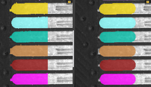
An image of connection slot pins. Some connections with pins are not covered with solder mask.
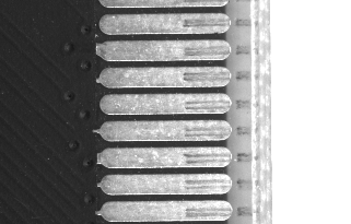
The input image is stored in
pcbdirectory.
Output
The count of pins with uncovered connections. The minimal area of uncovered connection should be 15 pixels.
Hints
The region of interest where uncovered elements can be found may be reduced. Only left part of pin can be analyzed.
To extract pins from the background, ThresholdToRegion filter can be used. Basic thresholding can be used because the color of pins is much brighter than the dark solder mask.
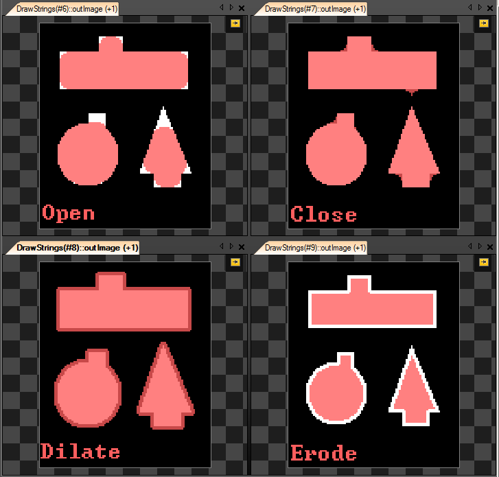
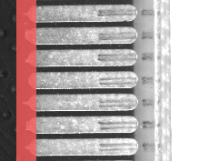
To find the defects it is necessary to use a region morphology operation. Results of some morphology operations are shown in the image below.
Labeling connections is explained in this article.
You can learn how to turn on sections here.
Solution (AVS)
-
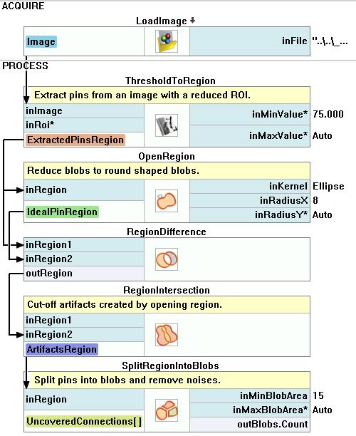
Load the image from a file using LoadImage.
-
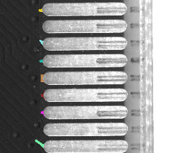
Extract pins from the image using ThresholdToRegion. Edit the inRoi input creating a region that covers the left side of the pins. Set inMinValue to 75.0:
-
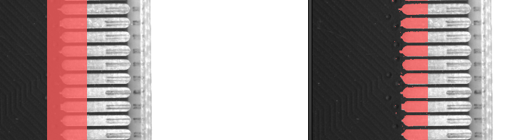
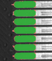
To get the PCB area without a covering, use the OpenRegion filter with the Ellipse mask and the input value of inRadiusX set to 8. The image below shows blobs before and after opening:
-
The resulting region is a difference between the found region and the region after opening. To get this region use the RegionDifference filter. The image below shows the region before opening (red) and the region after opening (green):
-
Opening the region allows to find the uncovered parts, but also creates some artifacts on the right side of the region. Remove the part of the region on the right and remove artifacts by adding the RegionIntersection filter. Find the intersection of the region with artifacts and a region which covers only the left ends of the pins:
-
The next step is to split the computed region using SplitRegionIntoBlobs with the minimal area of region equal to 15px.
-
To get the count of regions, expand Count field of input outBlobs in the SplitRegionIntoBlobs filter.
Macrofilter Main finds the uncovered parts of a PCB using basic Blob Analysis technique.
その他の資料
- ブロブ解析 - Article presents detailed information about the Blob Analysis technique.